What are the Raw Materials for PCBA
Printed circuit boards (PCBs) are made mostly of the following raw materials:
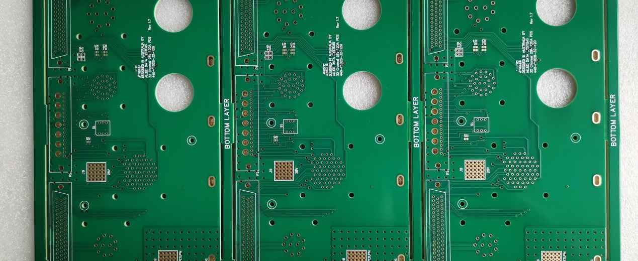
Substrate Material: The substrate, sometimes referred to as the base material or laminate, serves as the PCB’s structural backbone. In between the conducting layers, it offers insulation and mechanical support. The most used substrate material is an epoxy laminate reinforced with fibreglass called FR-4 (Flame Retardant 4). For particular uses, other materials including polyimide, FR-1, and FR-2 are also employed.
Copper Foil: The conductive traces on the PCB are made with copper foil. Typically, an adhesive layer is used to laminate it onto the substrate. Copper foil is available in several thicknesses, which are usually expressed in ounces per square foot (oz/ft2) or micrometres (μm), contingent on the specifications of the intended use.
Solder Mask: In order to avoid solder bridges and oxidation during assembly, a protective covering called a solder mask is placed over the copper traces. Usually, a liquid polymer resin is applied, and either heat or ultraviolet (UV) radiation is used to cure it.
Silkscreen Ink: Printing component outlines, logos, reference designators, and other identifying markers onto the PCB is done with silkscreen ink. It is usually applied by screen printing and can be made of a variety of materials, including inks based on acrylic or epoxy.
Surface Finish: To prevent oxidation and make soldering easier during assembly, surface finish compounds are applied to exposed copper surfaces. HASL (Hot Air Solder Leveling), ENIG (Electroless Nickel Immersion Gold), and OSP (Organic Solderability Preservatives) are examples of common surface treatments.
Solder Paste: During assembly, surface mount components are attached to the PCB using a mixture of flux and solder alloy particles called solder paste. Usually, a stencil is used to apply it to the PCB, and the solder is then heated to reflow and form a strong bond.
Adhesive: During the PCBA manufacturing process, adhesive compounds are employed to bind the layers together. They are frequently applied as thin films or sheets between layers and can have either an acrylic or epoxy basis.
Plating Chemicals: To make conductive traces and vias, copper is electroplated onto the substrate and through holes using plating chemicals. These substances usually consist of sulfuric acid, copper sulfate, and different additives to regulate the plating process.
Process of PCB’s Assembly
Printed circuit board (PCB) production usually entails a number of phases, including design, fabrication, assembly, and testing. Below is a summary of the overall procedure:
Design: Typically, specialist software like Altium Designer, Eagle, or KiCad is used for PCB design. After drawing out the circuit schematic, designers arrange the actual parts and traces on the board.
Generation of Gerber Files: The next stage after finishing the design is to create Gerber files. These files provide all the data needed to fabricate the PCB, such as drill holes, solder masks, and copper traces.
Material Selection: The electrical characteristics, mechanical strength, and cost of the PCB substrate are taken into consideration when making this choice. Fiberglass-reinforced epoxy, or FR-4, is a common material that is utilized extensively due to its balance of qualities.
Panelization: To streamline production and cut expenses, several PCBs are frequently assembled onto a single, bigger panel during fabrication.
Printing: A technique known as “printing” or “etching” is used to apply a coating of copper onto the substrate. Usually, a chemical etching procedure is used for this, in which a chemical solution selection
Drilling: To accommodate component leads and vias, holes are bored into the board. Precise hole drilling in accordance with design criteria is accomplished by automated drilling machines.
Through-Hole Plating (PTH): To establish electrical connections between the various PCB layers, a thin coating of conductive material—typically copper—is deposited inside the holes if the design calls for plated through-holes.
Application of Solder Mask: During assembly, a solder mask is placed over the copper traces to shield them from oxidation and to stop accidental solder bridges. Typically, the solder mask is applied using a photoresist technique, in which the mask material is selectively cured using UV radiation.
Silkscreen Printing: A technique called silkscreen printing is used to print logos, component outlines, reference designators, and other identifying markers onto PCBs.
Surface Finish: The surface finish of the PCB is applied to prevent oxidation of exposed copper traces and pads and to make soldering easier during assembly. HASL (Hot Air Solder Leveling), ENIG (Electroless Nickel Immersion Gold), and OSP (Organic Solderability Preservatives) are examples of common surface treatments.
Testing: To guarantee their quality and operation, the PCBs are put through a number of tests after they are manufactured. Functional testing, visual inspection, and electrical testing may be part of this.
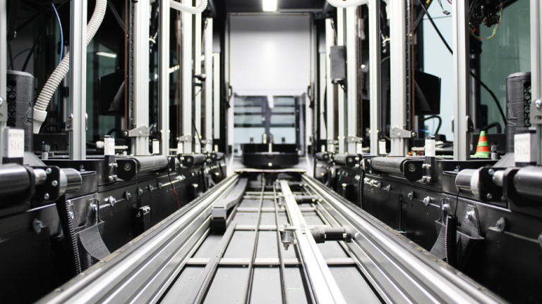
Assembly: Automated assembly machines are used to insert and solder components onto the PCB. Modern electronic components are often made using surface mount technology (SMT), however through-hole components are still utilized in select applications.
Final Testing: To ensure that every component is soldered correctly and that the circuit operates as intended, the assembled PCB is put through a final test.
Packing: After the PCBs pass the last round of testing, they are ready to be shipped to the client or integrated into bigger electrical systems.
Conclusion
A number of essential raw materials and procedures are used in the production of printed circuit boards (PCBs). The main raw materials are solder paste for component attachment, adhesive for layer bonding, substrate materials like FR-4, copper foil for conductive traces, solder mask for protection, silkscreen ink for labeling, and surface finish products for oxidation prevention. Functional printed circuit boards (PCBs) are made by carefully processing and assembling these materials during the manufacturing process, which includes phases like design, fabrication, assembly, and testing. Every step, from choosing the right substrate to applying solder pastes and surface treatments, is essential to guaranteeing the end product’s quality and functioning. In order to satisfy the various needs, these materials and processes must be carefully integrated.